ISSP workshop/ 物性研究所短期研究会

“Frontier of scanning probe microscopy and related nano science”
「機能的走査プローブ顕微鏡の新展開」

Date, Time (JST):

 March 30, 2022 (Wed.) 13:30-20:30
 March 31, 2022 (Thu.) 9:00-18:00

Registration deadline (JST):

 Poster presentation: March 23, 2022 (Wed.)
           Extended → March 28, 2022 (Mon.)
   Poster student award will be given.
   優秀な学生講演には賞が贈られます。

 Audience: March 31, 2022 (Thu.)

Registration fee:

 Free/無料

Venue:

 Online/ オンライン開催

Language:

 Hybrid of English and Japanese (depending on the session)
 セッション毎の日本語・英語のハイブリッド

Congratulations!

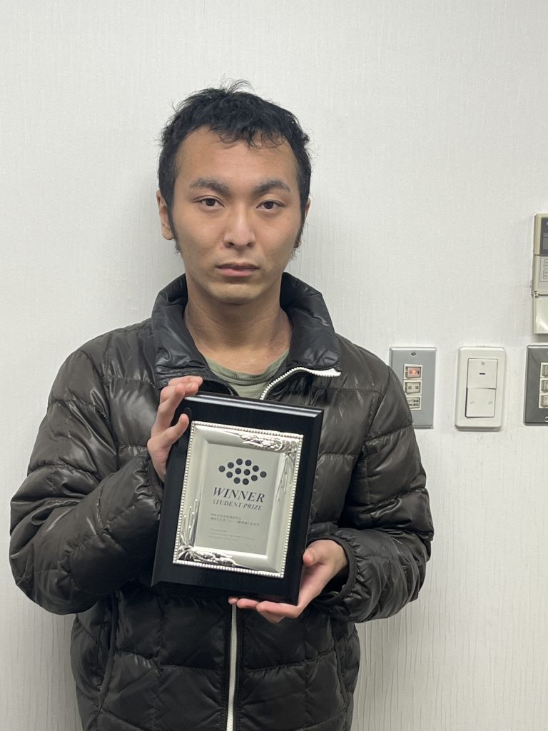
ポスター講演における学生賞を大阪大学の三坂朝基さんが受賞しました!

おめでとうございます!

Program


The assigned time is 30 minutes for your presentation + 10 minutes for discussion.
講演は、30分発表+10分討論を予定しています。

March 30, 2022 (Wed.)

13:30- 所長挨拶 森初果


Session1(Japanese/日本語)
Chair:Yukio Hasegawa (長谷川幸雄)

13:40-14:20 Kohei Yamasue (Tohoku Univ.)/山末 耕平 (東北大)

「時間分解SNDMを用いた半導体のナノスケール評価に関する最近の展開 」

Click to open the abstract/クリックして講演概要を開く
アブストラクト:走査型非線形誘電率顕微鏡(SNDM)は近接場マイクロ波を用いて探 針-試料間の静電容量変化を高感度に検出可能なプローブ顕微鏡である [1, 2].最 近,SNDMの拡張手法である時間分解SNDMが提案され,その半導体材料・デバイスの ナノスケール評価への応用が可能になっている [3].時間分解SNDMを用いること で,半導体のマクロな電気特性評価で用いられるDLTS(Deep level transient spectroscopy)や容量電圧(CV)特性測定をナノスケールで実現でき,界面欠陥密度分 布観察や多数キャリア密度分布とそのダイナミクスを可視化できる [4, 5, 6].本 講演ではパワーデバイス用新規材料であるSiC[4, 5]や原子層半導体のナノスケール 評価への応用など,最近の研究成果を述べる.

[1] Y. Cho, A. Kirihara, and T. Saeki, Rev. Sci. Instrum. 67, 2297-2303(1996).
[2] Y. Cho, Scanning Nonlinear Dielectric Microscopy: Investigation of Ferroelectric, Dielectric, and Semi-conductor Materials and Devices, Elsevier, ISBN 9780128172469 (2020).
[3] Y. Cho, Jpn. J. Appl. Phys. 56, 100101 (2017).
[4] Y. Yamagishi and Y. Cho, Appl. Phys. Lett. 111, 163103 (2017).
[5] K. Yamasue and Y. Cho, in 2021 IEEE International Symposium on the Physical and Failure Analysis of Integrated Circuits (IPFA) (2021).
[6] K. Suzuki, K. Yamasue, and Y. Cho, in 2019 IEEE International Integrated Reliability Workshop (IIRW) (2019).

14:20-15:00 Junsuke Yamanishi (IMS)/山西 絢介 (分子研)

「光誘起力顕微鏡に関する最近の動向 」

Click to open the abstract/クリックして講演概要を開く
光誘起力顕微鏡(PiFM)は探針と試料に光照射し、互いに生じる双極子間の相互作用力を検出することで試料の光学応答を観測するプローブ顕微鏡であり、2010年頃に初めて報告された[1]。光誘起の双極子間力は探針試料間距離に対して著しく減衰するために、PiFMは試料の光応答を数ナノメートルスケールで可視化することができる。これまで、単に光誘起の双極子間力を観測するに留まらず様々な分光測定(線形光学応答[2]、ラマン散乱[3]、過渡吸収[4]など)の研究が行われた。一方でPiFMには、光照射による探針及び試料の熱膨張が、光誘起の双極子間力の信号に混在してしまうという問題点がある[5]。本講演では、こういった最近の研究動向を踏まえ、その熱膨張の問題を解決した測定手法やそれを用いた観測に関する私の研究成果について述べる[6,7]。

[1] I. Rajapaksa et al., Appl. Phys. Lett. 97, 073121 (2010).
[2] J. Jahng et al., Acc. Chem. Res. 48, 2671 (2015).
[3] I. Rajapaksa et al., Appl. Phys. Lett. 99, 161103 (2011).
[4] J. Jahng et al., Appl. Phys. Lett. 106, 083113 (2015).
[5] J. Jahng et al., Anal. Chem. 90, 11054-11061 (2018).
[6] J. Yamanishi et al., Phys. Rev. Applied 9, 024031 (2018).
[7] J. Yamanishi et al., Nat. Commun. 12, 3865 (2021).

15:00-15:40 Yusuke Kajihara(Univ. Tokyo)/梶原 優介 (東京大)

「ナノサーモメトリーを実現するパッシブ近接場顕微鏡」

Click to open the abstract/クリックして講演概要を開く
物質表面には,伝導電子や格子振動など熱揺らぎに起因する正負電荷の相対運動が生じており,その時間変動電磁場によって強力な局在表面波が発現している.この局在表面波は熱励起エバネッセント波と呼ばれ,強力なエネルギーが表面から100 nm程度まで存在すること,常温では主要スペクトルがTHz帯(特に波長: 8~16 µm)に存在することが分かっている[1].熱励起エバネッセント波の強度は温度に依存するため,空間的に高分解能で計測可能であれば,「ナノスケールの熱分布」を計測できる.熱励起エバネッセント波の検出を実現するため,我々のグループでは超高感度のTHz検出器CSIP [2],共焦点光学系,およびプローブ顕微鏡を導入し,パッシブ型THz 近接場顕微鏡を構築している.先端径20 nm程度の近接場探針を測定対象の10 nm以下まで近づけ,探針先端でエバネッセント波を散乱させ,低温部(4.2 K)の検出器CSIPで検出する構成となっており,熱揺らぎを背景ノイズに埋もれさせないため,外部照射光を使っていない.構築顕微鏡を使用し,熱平衡状態において,常温物質からのエバネッセント波(波長: 14.5 µm)を空間分解能20 nmで検出している[3].本講演ではパッシブ近接場顕微鏡の概要や最近の研究成果[4,5]について紹介する.

[1] K. Joulain, J.P. Mulet, F. Marquier, R. Carminati, and J.J. Greffet, Surf. Sci. Rep. 57, 59 (2005).
[2] S. Komiyama, IEEE J. Sel. Top. Quantum Electron. 17, 54 (2011).
[3] Y. Kajihara, K. Kosaka, and S. Komiyama, Opt. Express, 19, 8, 7695 (2011).
[4] K-T. Lin, H. Nema, Q. Weng, S. Kim, K. Sugawara, T. Otsuji, S. Komiyama, and Y. Kajihara, Applied Physics Express, 13, 9 , (2020) 96501.
[5] R. Sakuma, K-T. Lin, S. Kim, F. Kimura, and Y. Kajihara, Rev. Sci. Instrum., 93 (2022) 13704.

Break/休憩


Session2(English)
Chair: Tetsuo Hanaguri (花栗哲郎)

16:00-16:40 Peter Liljeroth (Aalto University, Finland)

「Designer quantum states in van der Waals heterostructures」

Click to open the abstract/クリックして講演概要を開く
Van der Waals (vdW) heterostructures can be used to realize exotic quantum states not found in naturally occurring materials. I will describe our recent results on realizing topological superconductivity [1,2] and artificial heavy fermion systems in vdW heterostructures [3]. We use molecular-beam epitaxy (MBE) and low-temperature scanning tunneling microscopy (STM) for the sample growth and characterization. Topological superconductivity requires combining out of plane ferromagnetism, Rashba-type spin-orbit interactions and s-wave superconductivity, and we use monolayer ferromagnet CrBr3 on a superconducting NbSe2 substrate to realize this [1,2]. In the second part of the talk, I focus on our experiments on 1T-TaS2 / 1H-TaS2 heterostructures that bring together the building blocks of heavy fermion systems – Kondo coupling between a lattice of localized magnetic moments and mobile conduction electrons. These examples highlight the versatility of vdW heterostructures in realizing quantum states that are difficult to find and control in naturally occurring materials.

[1] S. Kezilebieke et al. Topological superconductivity in a van der Waals heterostructure, Nature 588, 424-428 (2020).
[2] S. Kezilebieke et al. Moiré-enabled topological superconductivity, Nano Lett. 22, 328 (2022).
[3] V. Vaňo et al. Artificial heavy fermions in a van der Waals heterostructure, Nature 599, 582-586 (2021).

16:45-17:25 Eli Zeldov (Weizmann Institute of Science, Israel)

「Nanoscale thermal imaging: Glimpse into dissipation in quantum systems down to atomic scale」

Click to open the abstract/クリックして講演概要を開く
Energy dissipation is a fundamental process governing the dynamics of classical and quantum systems. Despite its vital importance, direct imaging and microscopy of dissipation in quantum systems is currently mostly inaccessible because the existing thermal imaging methods lack the necessary sensitivity and are unsuitable for low temperature operation. We developed a scanning nanoSQUID that resides at the apex of a sharp pipette acting simultaneously as nanomagnetometer with single spin sensitivity and as nanothermometer providing cryogenic thermal imaging with four orders of magnitude improved thermal sensitivity of below 1 µK [1]. The non-contact non-invasive thermometry enables direct visualization and control of the minute heat generated by electrons scattering off a single atomic defect in graphene [2]. By further combining the scanning nanothermometry with simultaneous scanning gate microscopy we demonstrate independent imaging of work and dissipation and reveal the microscopic mechanisms that conceal the true topological protection in the quantum Hall state in graphene [3].

[1] D. Halbertal, J. Cuppens, M. Ben Shalom, L. Embon, N. Shadmi, Y. Anahory, H. R. Naren, J. Sarkar, A. Uri, Y. Ronen, Y. Myasoedov, L. S. Levitov, E. Joselevich, A. K. Geim, and E. Zeldov, Nature 539, 407 (2016).
[2] D. Halbertal, M. Ben Shalom, A. Uri, K. Bagani, A.Y. Meltzer, I. Marcus, Y. Myasoedov, J. Birkbeck, L.S. Levitov, A.K. Geim, and E. Zeldov, Science 358, 1303 (2017).
[3] A. Marguerite, J. Birkbeck, A. Aharon-Steinberg, D. Halbertal, K. Bagani, I. Marcus, Y. Myasoedov, A.K. Geim, D.J. Perello, and E. Zeldov, Nature 575, 628 (2019).

17:30-18:10 Milan P. Allan (Leiden University, Netherlands)

「Electron pairs without superconductivity in a disordered superconductor」

Click to open the abstract/クリックして講演概要を開く
The idea that preformed electron pairs could exist in a superconductor above its zero-resistance state has been explored for unconventional, interface, and disordered superconductors, yet direct experimental evidence is lacking. In this talk, I will introduce new instrumentation that can unambiguously detect and quantify the number of electron pairs in a sample: the electron pair microscope [1-3]. Applying it to the disordered superconductor titanium nitride, we show that the majority of electrons is paired up to temperatures much higher than the zero-resistance critical temperature Tc, by observing a clear enhancement in the shot noise that is equivalent to a change of the effective charge from 1 to 2 electron charges [4]. We further show that spectroscopic gap fills up rather than closes when increasing temperature. Our results thus demonstrate the existence of a novel state above Tc that, much like an ordinary metal, has no (pseudo)gap, but carries charge entirely via paired electrons.

[1] KM Bastiaans et al., RSI 89, 093709 (2018)
[2] KM Bastiaans, D. Cho et al., Nature Physics 14, 1183 (2018)
[3] KM Bastiaans et al., Phys. Rev. B 100, 104506 (2019)
[4] KM Bastiaans, et al. Science 374, 608 (2021)

Allanlab.org

18:10-20:30 poster session/ポスター講演


March 31, 2022 (Thu.)


Session3 (English)
Chair:Toshu An (安東秀)

9:00-9:40 Jiaqi Zhang (Japan Advanced Institute of Science and Technology, Japan)

「atomic scale mechanics studied by in-situ transmission electron microscopy with a quartz length-extension resonator」

Click to open the abstract/クリックして講演概要を開く
In this study, we developed an in-situ TEM holder equipped with a quartz resonator as force sensor to measure the mechanical properties of atomic scale materials when observing their atomic configurations. A quartz length-extension resonator (LER) was used to measure the stiffness of the materials by the frequency modulation method. The LER has the advantage to reduce its oscillation amplitude below 50 pm, thus we can observe atomic resolved TEM images under the condition of sensor oscillating. The stiffness of platinum (Pt) monatomic chains with 2-5 atoms were measured. The atomic resolution TEM images and videos were captured simultaneously with measuring the conductance and stiffness by our developed TEM holder. We investigated the stiffness of about 150 Pt monatomic chains for reproducibility and confirmed that the middle bond stiffness (25N/m) in the chain was slightly higher than that of the bond connect to the suspending tip (23N/m). In addition, the maximum elastic strain of individual bond in the chain is as large as 24%. These values are obviously different from the bulk counterpart. Such peculiar values can be briefly explained by the concept of “string tension”.

Group Homepage

9:45-10:25 Soohyon Phark (Institute for basic science, Korea)

「Atomic Scale Electron Spin Resonance: towards Electron Spin Qubits on a Surface」

Click to open the abstract/クリックして講演概要を開く
Scanning tunneling microscope (STM) equipped with pulsed electron spin resonance (ESR) enabled coherent spin control of individual atoms [1] and molecules [2] on surfaces. To date magnetic resonance in STM has relied on the modulation of the atomic scale local magnetic interaction between the spin and the STM tip [3,4,5], confining ESR in STM available for only one atom at a time. The poor coherence of the spins in the tunnel junction due to the tunneling electrons [1,2,6] severely restricts an application of the spins in STM to qubit control. Here, we introduce a new way of driving the magnetic resonance of a single atom in STM by the interaction with a single atom magnet in proximity. Pulsed ESR of a single Ti atom on MgO(100) with an Fe atom located in 5-10 Å away showed a non-vanishing Rabi rate ΩRabi, comparable with that driven by the interaction with the tip magnetic moment. We applied this new scheme to remotely drive magnetic resonance of a single atom positioned away from the tip, but weakly coupled with another atomic spin in the tunnel junction, which reads out the spin state of the “remote” spin. The spin-magnet pair provides a feasible building block of on-surface spin qubits, deserving a coherent control of multi qubits on a surface with an enhanced spin coherence.

[1] K. Yang et al. Science 366, 509-512 (2019).
[2] P. Willke et al. ACS Nano 15, 17959-17965 (2021).
[3] J. L. Lado et al. Phys. Rev. B 96, 205420 (2017).
[4] K. Yang et al. Phys. Rev. Lett. 122, 227203 (2019).
[5] J. R. Galvez et al. Phys. Rev. B 100, 035411 (2019).
[6] S. Phark et al. arXiv:2108.09880 (2021).

Break/休憩


Session4(日本語)
座長:Masahiro Haze (土師将裕)

10:50-11:30 Yuta Kainuma (JAIST)/貝沼 雄太(北陸先端大)

「走査ダイヤモンドNV中心プローブの開発と磁気イメージング 」

Click to open the abstract/クリックして講演概要を開く
ダイヤモンド中の窒素と空孔で構成されるNV(nitrogen-vacancy)中心は室温で単一のNV中心のESR(electron spin resonance)を光学的に検出可能であり、NV中心のスピン状態が長いコヒーレンス時間を有することから量子制御も可能である。また、NV中心は高い磁場感度(DC: 2 µT/Hz1/2, AC: 18 nT/Hz1/2)1を有し、原子サイズであることより走査磁気プローブ顕微鏡に応用されてきた1。さらには、磁気イメージングにおいて、スピン位相緩和やスピン格子緩和などの時間分解計測法を用いることで単一スピンのイメージングや金属中のジョンソンノイズの計測による伝導率のイメージング等も報告されている2。近年では、スピン波の検出・イメージングも実証され、スピントロニクス分野への貢献が期待される3,4,5。 本講演では、走査ダイヤモンドNV中心プローブの作製法と磁気イメージングに関する報告6とこの分野の今後の展望について紹介する。

1 M.S. Grinolds, S. Hong, P. Maletinsky, L. Luan, M.D. Lukin, R.L. Walsworth, and A. Yacoby, Nat. Phys. 9, 215 (2013).
2 A. Ariyaratne, D. Bluvstein, B.A. Myers, and A.C.B. Jayich, Nat. Commun. 9, 2406 (2018).
3 D. Kikuchi, D. Prananto, K. Hayashi, A. Laraoui, N. Mizuochi, M. Hatano, E. Saitoh, Y. Kim, C.A. Meriles, and T. An, Appl. Phys. Express 10, 103004 (2017).
4 D. Prananto, Y. Kainuma, K. Hayashi, N. Mizuochi, K.I. Uchida, and T. An, Phys. Rev. Appl. 16, 064058 (2021).
5 T.X. Zhou, J.J. Carmiggelt, L.M. Gächter, I. Esterlis, D. Sels, R.J. Stöhr, C. Du, D. Fernandez, J.F. Rodriguez-Nieva, F. Büttner, E. Demler, and A. Yacoby, Proc. Natl. Acad. Sci. U. S. A. 118, e2019473118 (2021).
6 Y. Kainuma, K. Hayashi, C. Tachioka, M. Ito, T. Makino, N. Mizuochi, and T. An, J. Appl. Phys. 130, 243903 (2021).

研究室HP  研究室Twitter

11:35-12:15 Takashi Kumagai (IMS)/熊谷 崇(分子研)

「原子スケールの極微分光」

Click to open the abstract/クリックして講演概要を開く
走査プローブ顕微鏡とプラズモニクスの融合によってナノスケール、さらには一原子・一分子レベルの極微分光が可能となってきました。講演では私たちの研究グループの最近の成果を中心として原子スケールの極微分光について紹介する予定です。研究の詳細については以下のオープンアクセス論文もご参照ください。

1. B. Cirera et al. Charge Transfer-Mediated Dramatic Enhancement of Raman Scattering upon Molecular Point Contact Formation. Nano Letters
2. S. Liu et al. Anti-Stokes Light Scattering Mediated by Electron Transfer Across a Biased Plasmonic Nanojunction. ACS Photonics 8, 2610–2617 (2021).
3. S. Liu et al. Atomic Point Contact Raman Spectroscopy of a Si (111)-7× 7 Surface. Nano Letters 21, 4057–4061 (2021).
4. S. Liu et al. Dramatic Enhancement of Tip-Enhanced Raman Scattering Mediated by Atomic Point Contact Formation. Nano Letters 20, 5879–5884 (2020).
5. S. Liu et al. Resolving the Correlation between Tip-Enhanced Resonance Raman Scattering and Local Electronic States with 1 nm Resolution, Nano Letters 19, 5725–5731 (2019).
6. H. Böckmann et al. Near-Field Manipulation in a Scanning Tunneling Microscope Junction with Plasmonic Fabry-Pérot Tips. Nano Letters 19, 3597–3602 (2019).
7. H. Böckmann et al. Near-Field Spectral Response of Optically Excited Scanning Tunneling Microscope Junctions Probed by Single-Molecule Action Spectroscopy. J. Chem. Phys. Lett. 10, 2068–2074 (2019).
8. H. Böckmann et al. Near-Field Enhanced Photochemistry of Single Molecules in a Scanning Tunneling Microscope Junction. Nano Letters 18, 152–157 (2018).

Break/休憩


Session4(日本語)
座長:Yoshiaki Sugimoto (杉本宜昭)

13:30-14:10 Takeshi Fukuma (Kanazawa Univ.)/福間 剛士(金沢大)

「AFMによる3次元自己組織化構造の内部観察」

Click to open the abstract/クリックして講演概要を開く
原子間力顕微鏡(AFM)は、元来表面の凹凸を探針でなぞることで2次元画像として可視化する技術であった。一方、液中においては様々な液体や分子鎖、イオンなどが複雑に相互作用して3次元自己組織化構造を作り出し、多彩な機能を発現している。これらの内部は従来のAFMでは、観察できなかったが、近年、探針を3次元的に走査し、その間に探針が受ける力を可視化する3次元AFMの登場により、その状況は一変しつつある。これまでに、様々な研究グループの手によって、鉱物や生体試料の表面における3次元水和構造が可視化されてきた。それに加えて、我々は同様の原理が多様な自己組織化構造の可視化に応用できる可能性に着目し、その検証に取り組んできた。これまでに、脂質分子頭部の揺動構造や、ハードディスク表面の分子吸着構造、イオン液体/電極界面の液体構造、高分子/水界面の水和膨潤構造、さらには生細胞内部のナノ構造など、サブナノスケールからマイクロメータスケールに及ぶ多様な構造の可視化を示してきた。本講演では、これらの3次元AFMによる液中3次元自己組織化構造の可視化に関する最新の研究成果について報告する。

1. Penedo, M.; Miyazawa, K.; Okano, N.; Furusho, H.; Ichikawa, T.; Alam Mohammad, S.; Miyata, K.; Nakamura, C.; Fukuma, T., Visualizing intracellular nanostructures of living cells by nanoendoscopy-AFM. Sci. Adv. 2021, 7 (52), eabj4990.
2. Fukuma, T.; Garcia, R., Atomic- and Molecular-Resolution Mapping of Solid-Liquid Interfaces by 3D Atomic Force Microscopy. ACS Nano 2018, 12 (12), 11785-11797.
3. Asakawa, H.; Yoshioka, S.; Nishimura, K.; Fukuma, T., Spatial Distribution of Lipid Headgroups and Water Molecules at Membrane/Water Interfaces Visualized by Three-Dimensional Scanning Force Microscopy. ACS Nano 2012, 6 (10), 9013-9020.

研究室HP   研究所HP

14:15-14:55 Norio Okabayashi (Kanazawa Univ.)/岡林 則夫(金沢大)

「外場による単一分子の構造変化とエネルギー散逸」

Click to open the abstract/クリックして講演概要を開く
金属表面上の一酸化炭素(CO)分子とプローブ顕微鏡の金属探針との相互作用は、subatomic分解能やCO修飾探針の結像原理との関連から重要な課題となっている[1]。我々は、この問題を解明するために、走査型トンネル顕微鏡と原子間力顕微鏡を組み合わせ、探針の作る力場とCO分子の振動エネルギーの関係を調べてきた[2-4]。そして探針からの引力が増加すると、振り子に対応する振動モードのエネルギーが増加することを見出した[3]。その後、力が斥力に至る領域まで実験を拡張し、更に密度汎関数法を用いた理論計算を取り入れた。そして、(1)力が引力から斥力に変わると振り子モードの振動エネルギーが減少すること、(2)斥力が強くなるとCO分子にとって安定なサイトがトップサイトからブリッジサイトに変わること、(3)探針を表面に近づけ遠ざけることを繰り返すと、分子がトップサイトとブリッジサイトの間を行き来し、その際にエネルギーの散逸が観測されることを見出した[5]。更に、このようなブリッジサイトにおけるCO分子の吸着が探針による分子操作とその際に発生する動摩擦を理解するうえで重要であることを見出した[5]。

[1] F. J. Giessibl, Rev. Sci. Instrum. 90, 011101 (2019)
[2] N. Okabayashi et al., PRB 93, 165415 (2016).
[3] N. Okabayashi, A. Peronio, M. Paulsson, T. Arai, and F. J. Giessibl, PNAS. 115, 4571 (2018).
[4] A. Peronio, N. Okabayashi, F. Griesbeck, F. Giessibl, Rev. Sci. Instrum. 90, 123104 (2019).
[5] N. Okabayashi, T. Frederiksen, A. Liebig, F. J. Giessibl. arXiv:2112.12286

研究者HP

15:00-15:40 Hiroyuki Koshida (Univ. Tokyo)/越田 裕之(東京大)

「金属表面におけるNOの吸着状態と磁性」

Click to open the abstract/クリックして講演概要を開く
一酸化窒素 (NO) は最外殻軌道である2π*軌道に局在する不対電子に起因した,スピン磁気モーメントを有している二原子分子である。NOは最も単純な磁性分子と見なすことができるため,基礎的な観点から,表面に吸着したNOの磁性は関心を集めている [1]。しかし多くの系において,NOの2π*軌道は吸着によって表面電子系と強く混成し化学結合を形成するため,局在スピンは消失する。そのため,表面系におけるNOのスピン検出の報告は,Au(111)表面における一例 [2] に限られており,NOの表面磁性に関する知見は限られていた。本講演では,われわれが近年取り組んだ,走査トンネル顕微鏡/分光 (STM/STS)によるAu(110)-(1×2)表面におけるNOの吸着状態と電子・スピン状態の相関測定 [3] を紹介し,「最小の磁性分子」の一つであるNOのふるまいを論じる。

[1] A. Yoshimori. Surf. Sci., 342(1-3):L1101–L1103, 1995.
[2] R. Requist et al. Proc. Natl. Acad. Sci. USA, 111(1):69–74, 2014.
[3] H. Koshida et al. Phys. Rev. B 103.15 (2021): 155412.

Break/休憩


Session5(日本語)
座長: Masahiro Haze (土師将裕)

16:00-16:40 Koichiro Ienaga (Tokyo Tech.)/家永 紘一郎(東工大)

「単層近藤格子CePt2/Pt(111)の成長と電子状態」

Click to open the abstract/クリックして講演概要を開く
Ce系,U系化合物に代表される近藤格子系では,f電子軌道と伝導電子の混成の強さに応じてコヒーレント近藤状態,磁気秩序,超伝導といった多彩な電子相関現象が生じる.これらの物質群を低次元化すると電子状態が劇的に変わることが,エピタキシャル成長させた交代積層格子の輸送特性から明らかにされている[1].そこで我々は,膜厚などの構造パラメータを制御しながら表面からの構造/電子状態観察が可能な系として,Pt(111)基板上にエピタキシャル成長されたCePt5 [2]に着目した.CePt5 はPt3層とCePt2層の積層からなり,多層膜CePt5/Pt(111)では20 K以下でコヒーレント近藤状態を形成することが角度分解光電子分光によって示唆されている[3].しかし,単層膜の成長可能性や構造に関してはコンセンサスが得られておらず,詳細な電子状態観測の報告もない.そこで,CePt5の単層膜をPt(111)上へ成長させ,走査トンネル顕微/分光法で構造と電子状態を観察した[4].原子分解能観察から,最表面層に(2×2)Pt4層をもつ単原子層CePt2の形成が判明した.5 Kでの準粒子干渉測定ではPt表面状態の下方シフトが観測され,表面直下のCePt2層から表面Pt4層への電荷移動と解釈される.さらに分光測定ではコヒーレント近藤状態を示唆する異常が観測された.

[1] H. Shishido, T. Shibauchi, K. Yasu, T. Kato, H. Kontani, T. Terashima, Y. Matsuda, Science 327, 980 (2010).
[2] J. Kemmer, C. Praetorius, A. Krönlein, P.-J. Hsu, K. Fauth, and M. Bode, Phys. Rev. B 90, 195401 (2014).
[3] M. Klein et al., Phys. Rev. Lett. 106, 186407 (2011).
[4] K. Ienaga, S. Kim, T. Miyamachi, and F. Komori, Phys. Rev. B 104, 165419 (2021).

研究室HP

16:45-17:25 Tomoya Asaba (Kyoto Univ.)/浅場 智也(京都大)

「 チューリング不安定性による原子スケールワイヤおよびジャンクションの作製 」

Click to open the abstract/クリックして講演概要を開く
原子スケールで均一なワイヤを成長させ、ネットワークを構築することはナノテクノロジーにおける重要な課題である。本研究では、原子レベルで滑らかなX、Y接合やナノリングを含む様々な配置の原子スケールワイヤを作製するための簡単な方法を発見した。具体的には、beta-RuCl3をパルスレーザー堆積法でグラフェンおよびグラファイト表面上に蒸着することにより、原子スケールワイヤから形成されるパターンを成長させた。走査型トンネル顕微鏡による測定から、ワイヤの高さは0.6ナノメートル、幅は1.4 および2.8 nmで一定であり、また数マイクロメートルの長さをもっていることがわかった。さらに、ワイヤの間隔は均一であり、数ナノメートルから数十ナノメートルの間で調節可能である。一方でこのパターンの生成メカニズムに着目すると、ターゲットパターンやスパイラルパターンといった非平衡反応拡散過程に特徴的な構造が観測された。これらの結果は、チューリング不安定性が原子ワイヤとそのネットワーク構造の自己形成に関与していることを示す。今回の発見は、ナノネットワーク作製へのユニークな道を開くとともに、原子スケールでの非平衡自己組織化現象に新しい視点を提供するものである。

17:30- Closing

Registration

締めきりました

Sponsored by:

 Institute for Solid State Physics, University of Tokyo
 東京大学物性研究所

Co-sponsored by:

 Scanning probe microscopy committee in the Japan Society of Vacuum and Surface Science
 日本表面真空学会走査プローブ顕微鏡研究部会
 

Committee members:

 Toshu An (JAIST)/安東秀(北陸先端大)
 Yousoo Kim (RIKEN)/金有洙(理研)
 Tetsuo Hanaguri (RIKEN)/花栗哲郎(理研)
 Yukio Hasegawa (Univ. Tokyo)/長谷川幸雄(東京大)
 Masahiro Haze (Univ. Tokyo)/土師将裕(東京大)
 Yoshinori Okada (OIST)/岡田佳憲(沖縄科技大)
 Yoshiaki Sugimoto (Univ. Tokyo)/杉本宜昭(東京大)
 Yasuo Yoshida (Kanazawa Univ.)/吉田靖雄(金沢大)

For further questions, please contact to Masahiro Haze (haze -at- issp.u-tokyo.ac.jp).
Please replace -at- to @.
お問い合わせは土師(haze -at- issp.u-tokyo.ac.jp)まで。
-at-を@に置き換えてください。