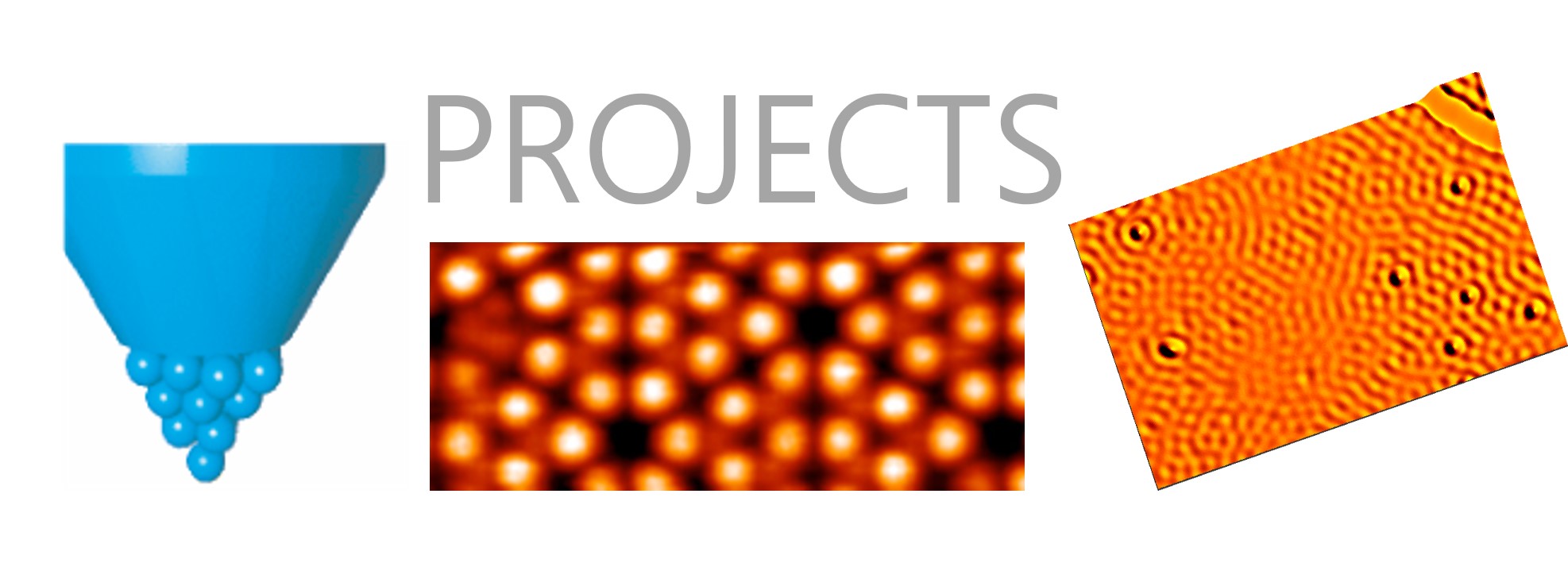
ťē∑Ťį∑Ś∑ĚÁ†ĒÁ©∂Śģ§„Āß„ĀĮ„ÄĀŤĶįśüĽ„Éą„É≥„Éć„Éęť°ēŚĺģťŹ°ÔľąÔľ≥ÔľīÔľ≠ԾȄāíšĹŅ„Ā£„Ā¶„ÄĀŤ°®ťĚĘšłä„Āß„Āģ„Éä„Éé„āĻ„āĪ„Éľ„Éę„Āß„ĀģŤß£śėé„āíťÄ≤„āĀ„Ā¶„ĀĄ„Āĺ„Āô„Äā
Ôľ≥ÔľīÔľ≠„ĀĮ„ÄĀśéĘťáĚÔľą„Éó„É≠„Éľ„ÉĖԾȄĀ®ŚĎľ„Āį„āĆ„āčťáĚ„ā퍶≥ŚĮü„Āó„Āü„ĀĄŤ©¶śĖôŤ°®ťĚĘ„ĀęŤŅĎ„Ā•„ĀĎ„ÄĀŤ°®ťĚĘ„āí„Ā™„Āě„āč„Āď„Ā®„Āę„āą„Ā£„Ā¶Ť°®ťĚĘ„ĀģŚáĻŚáł„ā퍶č„āčť°ēŚĺģťŹ°„Āß„Āô„ÄāťáĚ„Ā®Ť©¶śĖô„Ā®„ĀģťĖď„ĀęśĶĀ„āĆ„āč„Éą„É≥„Éć„ÉęťõĽśĶĀ„ā팹©ÁĒ®„Āô„āč„Āď„Ā®„Āę„āą„Ā£„Ā¶„ÄĀťáĚ„āíŚéüŚ≠źśēįŚÄ茹܄ĀĽ„Ā©ťõĘ„āĆ„ĀüšĹćÁĹģ„ĀęšŅĚśĆĀ„Āó„Ā™„ĀĆ„āČ„Ā™„Āě„āč„Āď„Ā®„ĀĆ„Āß„Āć„āč„Āģ„Āß„ÄĀŤ°®ťĚĘšłä„ĀģŚéüŚ≠ź„āĻ„āĪ„Éľ„Éę„ĀģŚáĻŚáł„ÄĀ„Āô„Ā™„āŹ„Ā°ŚéüŚ≠źŚÉŹ„āíśíģ„āč„Āď„Ā®„ĀĆ„Āß„Āć„Āĺ„Āô„ÄāŤĶįśüĽ„Éą„É≥„Éć„Éꌹ܌ÖČÔľąÔľ≥ÔľīÔľ≥)„Ā®ŚĎľ„Āį„āĆ„āčśČčś≥ē„āíšĹĶÁĒ®„Āô„āĆ„Āį„ÄĀťáĚÁõīšłč„ĀģŤ©¶śĖôŤ°®ťĚĘ„Āß„ĀģťõĽŚ≠źÁä∂śÖč„ĀęťĖĘ„Āô„āčśÉÖŚ†Ī„āāŚĺó„āč„Āď„Ā®„āā„Āß„Āć„Āĺ„Āô„Äā
ťē∑Ťį∑Ś∑ĚÁ†ĒÁ©∂Śģ§„Āß„ĀĮÁČĻ„Āę„ÄĀšĹéśł©„ÉĽÁ£ĀŚ†īšł≠„ÉĽRFÁíįŚĘÉšłč„Ā™„Ā©„ĀģÁČĻśģäÁíįŚĘÉšłč„Āß„Āģ Á≤ĺŚļ¶„Āģťęė„ĀĄśł¨Śģö„Āę„Āď„Ā†„āŹ„Ā£„Ā¶„Āä„āä„ÄĀ šĽĖ„ĀģśČčś≥ē„Āß„ĀĮŚĺó„āČ„āĆ„Ā™„ĀĄÁŹĺŤĪ°„ĀģŤ¶≥śł¨„āíÁõģśĆá„Āó„Ā¶„ĀĄ„Āĺ„Āô„Äā
„Āď„Āď„Āęśõł„Āč„āĆ„Ā¶„ĀĄ„āčÁ†ĒÁ©∂ŚÜÖŚģĻ„ĀģšĽĖ„Āę„āā„ÄĀśßė„ÄÖ„Ā™ŚÖĪŚźĆÁ†ĒÁ©∂„āĄŤ£ÖÁĹģťĖčÁôļ„Ā™„Ā©„āāŤ°Ć„Ā£„Ā¶„ĀĄ„Āĺ„Āô„Äā
We are working on studies of surface science in nanometer scale using scanning tunneling microscopy (STM).
STM detects a topography by scanning a very sharp tip closely above a sample surface. Tip-sample distance can be stabilized by detecting tunneling current which changes dramatically depending on the tip-sample distance. By scanning tunneling spectroscopy (STS), we can get information about electronic states in atomic scales.
Especially, we focus on precise measurements in extreme conditions, such as low temperature, high magnetic field, RF electromagnetic field.
Besides the above subjects, we are working on various joint researches and system developments.
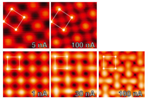
1. Ť°®ťĚĘšļĆś¨°ŚÖÉťõĽŚ≠źÁ≥Ľ„ĀģÁČ©śÄߍ¶≥śł¨ (Electronic states of two dimensional systems)
Ť°®ťĚĘśēįŚéüŚ≠źŚĪ§„ĀęŚĪÄŚú®„Āó„ĀüťõĽŚ≠źÁä∂śÖč„āíśĆĀ„Ā§Ť°®ťĚĘÁ≥Ľ„ā팹©ÁĒ®„Āó„Ā¶šļĆś¨°ŚÖÉťõĽŚ≠źÁ≥Ľ„ĀęťĖĘ„Āô„āč„Āē„Āĺ„ĀĖ„Āĺ„Ā™ÁŹĺŤĪ°„ĀģŚģüÁ©ļťĖ≥ŚĮü„āíÁõģśĆá„Āó„Ā¶„ĀĄ„Āĺ„Āô„Äā
ŚĮĺŤĪ°„ĀĮ„ÄĀŚźłÁĚÄŚéüŚ≠ź„Ā™„Ā©Ť°®ťĚĘśßčťÄ†„Ā®„ĀģÁõłšļíšĹúÁĒ®„ÄĀťĖČ„ĀėŤĺľ„āĀŚäĻśěú„ÄĀťõĽŚ≠źŚģöŚú®ś≥Ę„ÉĽ„Éē„É™„Éľ„Éá„ÉęśĆĮŚčē„ÉĽťĀģŤĒĹŚäĻśěú„ÄĀ„Éē„ā©„Éé„É≥„Ā®„ĀģÁõłšļíšĹúÁĒ®„Āę„āą„āč„Éē„āß„Éę„ÉüťĚĘŤŅĎŚāć„ĀģťõĽŚ≠źÁä∂śÖč„ÄĀŤŅĎŤó§ŚäĻśěú„Ā™„Ā©„Ā™„Ā©„ÄĀšĹéśł©Ôľąś∂≤šĹď„Éė„É™„ā¶„ɆԾȍ∂ÖťęėÁúüÁ©ļŤĶįśüĽ„Éą„É≥„Éć„Éęť°ēŚĺģťŹ°ÔľąÔľ≥ÔľīÔľ≠ԾȄāíÁĒ®„ĀĄ„Āü„Éą„É≥„Éć„Éꌹ܌ÖČ„Āę„āą„āčťęėÁ≤ĺŚļ¶„Āß„ĀģťõĽŚ≠źÁä∂śÖčśł¨ŚģöśäÄŤ°ď„ĀĆťćĶ„Ā®„Ā™„āä„Āĺ„Āô„Äā
We are working on real space measurements of electronic systems confined in a few atomic layers.
Our interests are various phenomena of surface, such as interactions between substrates and adatoms, standing waves, Friedel oscillations, shielding effects, electron-phonon interactions, and Kondo effects.
Ultrahigh vacuum and low temperature conditions are the key role to reveal high resolution STM measurements.
References:
M. Ono et al.,Appl. Surf. Sci. 256, 469-474 (2009)
M. Ono et al.,Phys. Rev. Lett. 96, 016801 (2006)
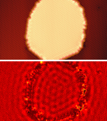
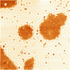
2. „Éä„Éé„āĶ„ā§„āļŤ∂ÖšľĚŚįéšĹď (Nano-sized superconducting materials)
„ā∑„É™„ā≥„É≥ŚüļśĚŅšłä„ĀęŤ∂ÖšľĚŚįéšĹď„Āß„Āā„āčťČõ„āíŤíłÁĚÄ„Āô„āč„Āď„Ā®„Āę„āą„Ā£„Ā¶„ÄĀ„āĘ„ā§„É©„É≥„ÉČśßčťÄ†„āĄŚćėŚĪ§Ť∂ÖšľĚŚįéŤĖĄŤÜú„āíšĹúŤ£Ĺ„Āó„ÄĀ„ĀĚ„ĀģŤ∂ÖšľĚŚįéÁČĻśÄß„āí„Éą„É≥„Éć„Éꌹ܌ÖČśł¨Śģö„Āę„āą„ā䍩ēšĺ°„Āó„Ā¶„ĀĄ„Āĺ„Āô„Äā„āĶ„ā§„āļ„ÉĽŚĹĘÁä∂šĺĚŚ≠ėśÄß„āĄÁ£ĀŚ†īšł≠„Āß„ĀģÁ£ĀśĚü„ĀģšĺĶŚÖ•ÁČĻśÄß„ÄĀ„ĀĚ„Āó„Ā¶ŚłłšľĚŚįéšĹď„Āł„ĀģŤ∂ÖšľĚŚįéÁČĻśÄß„Āģ„Āó„ĀŅŚáļ„Āó„ĀꍹąŚĎ≥„āíśĆĀ„Ā£„Ā¶Á†ĒÁ©∂„ā퍰ƄĀ£„Ā¶„ĀĄ„Āĺ„Āô„ÄāšłĖÁēĆ„Āß„āāÁ®ÄŚįĎ„Ā™„Éė„É™„ā¶„ɆԾďŚÜ∑ŚćīÔľąŚąįťĀĒśł©Śļ¶ÔľźÔľéÔľĒԾꚼ•šłčԾȄĀģŤ∂ÖťęėÁúüÁ©ļÔľ≥ÔľīÔľ≠„Āę„āą„āäśł¨Śģö„Āó„Ā¶„Āä„āä„ÄĀÔĹćÔĹÖÔľ∂šĽ•šłč„ĀģÁ≤ĺŚļ¶„Āß„ĀģŤ®ąśł¨„ĀĆŚŹĮŤÉĹ„Āß„Āô„Äā
We are interested in superconducting properties of nano sized island and films of superconductors (e.g., Pb). Superconducting properties, such as formation of vortices, proximity effect, and critical field) depending on size and shape are studied by low temperature (~0.4K) and ultrahigh vacuum STM.
References:
H. Kim et al.,Phys. Rev. Lett. 117, 116802 (2016)
H. Kim and Y. Hasegawa Phys. Rev. Lett. 114, 206801 (2015).
„Ā™„Ā©
3. Ť°®ťĚĘŚźłÁĚÄŚąÜŚ≠ź„ĀģÁ£ĀśÄß„Ā®„āĻ„ÉĒ„É≥ŚĀŹś•ĶSTM (Magnetic molecules studied by spin-polarized STM)
Á£ĀśÄßśéĘťáĚ„āíÁĒ®„ĀĄ„Ā¶Á£ĀśÄߍ°®ťĚĘ„āíśł¨Śģö„Āô„āč„Ā®„ÄĀ„Éą„É≥„Éć„ÉęÁ£ĀśįóśäĶśäóŚäĻśěú„Āę„āą„Ā£„Ā¶śéĘťáĚ„Ā®„āĶ„É≥„Éó„Éę„ĀģÁ£ĀŚĆĖ„ĀģŚźĎ„Āć„ĀęšĺĚŚ≠ė„Āó„Ā¶„Éą„É≥„Éć„ÉęťõĽśĶĀ„ĀĆŚ§ČŚĆĖ„Āô„āč„Āü„āĀ„Āę„ÄĀŤ°®ťĚĘ„Āę„Āä„ĀĎ„āčÁ£ĀśįóśßčťÄ†„āíŚéüŚ≠ź„āĻ„āĪ„Éľ„Éę„Āߍ©≥Áīį„ĀꍙŅ„ĀĻ„āč„Āď„Ā®„āāŚŹĮŤÉĹ„Ā®„Ā™„āä„Āĺ„Āô„Äā„Āĺ„Āü„ÄĀŤ°®ťĚĘ„Éä„ÉéÁ£ĀśÄßšĹď„ĀęŚĮĺ„Āó„Ā¶śßė„ÄÖ„Ā™Á£ĀŚ†ī„Āßśł¨Śģö„ā퍰ƄĀÜ„Āď„Ā®„Āß„ÄĀ„ĀĚ„ĀģÁ£ĀśÄßšĹď„ĀģÁ£ĀŚĆĖśõ≤Á∑ö„ā휏Ź„ĀŹ„Āď„Ā®„āāŚŹĮŤÉĹ„Āß„Āô„ÄāÁŹĺŚú®„ĀĮ„ÄĀ„ĀĚ„ĀģŚĮĺŤĪ°„Ā®„Āó„Ā¶Á£ĀśÄߌąÜŚ≠ź„ĀꍹąŚĎ≥„āíśĆĀ„Ā£„Ā¶Á†ĒÁ©∂„ā퍰ƄĀ£„Ā¶„ĀĄ„Āĺ„Āô„ÄāśúÄÁĶāÁöĄ„Āę„ĀĮ„ÄĀ„āĻ„ÉĒ„É≥ŚĀŹś•ĶSTM„Ā®ŚąÜŚ≠ź„Éě„Éč„ÉĒ„É•„ɨ„Éľ„ā∑„Éß„É≥„āíÁĶĄ„ĀŅŚźą„āŹ„Āõ„Ā¶„ÄĀšĹ霨°ŚÖɝᏌ≠ź„āĻ„ÉĒ„É≥Á≥Ľ„ā퍰®ťĚĘšłä„Āßśßčśąź„Āó„ÄĀ„ĀĚ„ĀģťáŹŚ≠źÁ£ĀśÄß„ā퍙Ņ„ĀĻ„āč„Āď„Ā®„āíÁõģśĆá„Āó„Ā¶„ĀĄ„Āĺ„Āô„Äā
When a magnetic tip is used for scanning, sample magnetic structures in nanoscale can be investigated by detecting tunneling magnetoresistance between a tip and a sample. In addition, magnetization curve can be measured in magnetic fields. We are interested in magnetic molecules, taking into consideration to build up a low dimensional system by the atomic/molecule manipulation technique.
Á†ĒÁ©∂śąźśěúÔľö
S. Yamamoto et al.,Phys. Rev. B 93, 081408(R) (2016)
„Ā™„Ā©
4. „āĻ„ÉĒ„É≥ŚĀŹś•ĶSTM„Āę„āą„āčťáćŚÖÉÁī†ŚüļśĚŅšłä„Āģ3dÁ£ĀśÄßťáĎŚĪěŤĖĄŤÜú„ĀģÁ†ĒÁ©∂ (Chiral magnetism studied by spin-polarized STM)
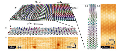
ťáć„ĀĄŚüļśĚŅšłä„ĀģÁ£ĀśÄߍĖĄŤÜú („āŅ„É≥„āį„āĻ„ÉÜ„É≥Ť°®ťĚĘšłä„Āģ3dÁ£ĀśÄßťáĎŚĪěŤĖĄŤÜú„Ā™„Ā©) „ĀĮ„ÄĀ„āł„É£„É≠„ā∑„É≥„āĻ„ā≠„ÉľŚģąŤį∑ÁõłšļíšĹúÁĒ®„Āę„āą„Ā£„Ā¶Ť§áťõĎ„Ā™Á£ĀśįóśßčťÄ†„ĀĆÁŹĺ„āĆ„Āĺ„Āô„ÄāśąĎ„ÄÖ„ĀĮ„āĻ„ÉĒ„É≥ŚĀŹś•ĶSTM„Āę„āą„Ā£„Ā¶„ĀĚ„ĀģÁ£ĀśįóśßčťÄ†„āĄŚäĪŤĶ∑Áä∂śÖč„ĀģÁ†ĒÁ©∂„ĀꌏĖ„āäÁĶĄ„āď„Āß„ĀĄ„Āĺ„Āô„Äā
Complex magnetic structures appear due to the Dzyaloshinskii-Moriya interaction on magnetic thin films formed on heavy metals, such as 3d magnetic metal thin films on a tungsten substrate. We study the magnetic structures and excitation state in a nanometer scale.
Á†ĒÁ©∂śąźśěúÔľö
M. Haze et al., Sci. Rep. 7, 13269 (2017).
M. Haze et al., Phys. Rev. B 95, 060415(R) (2017).
„Ā™„Ā©
5. ťáć„ĀĄťõĽŚ≠źÁ≥ĽŤ∂ÖšľĚŚįéšĹď„ĀģSTM/STS (STM/STS studies of heavy fermion materials)
BCSÁźÜŤęĖ„Āß„ĀĮŤ™¨śėé„Āô„āč„Āď„Ā®„ĀĆ„Āß„Āć„Ā™„ĀĄÁ£ĀśÄß„Ā®ŚÖĪŚ≠ė„Āô„āčÁČĻÁēį„Ā™Ť∂ÖšľĚŚįéšĹď„ĀęŚĮĺ„Āó„ÄĀ„Éė„É™„ā¶„ɆԾďŚÜ∑ŚćīÔľąŚąįťĀĒśł©Śļ¶ÔľźÔľéÔľĒԾꚼ•šłčԾȄĀģŤ∂ÖťęėÁúüÁ©ļÔľ≥ÔľīÔľ≠„āíÁĒ®„ĀĄ„Ā¶ŤĶįśüĽ„Éą„É≥„Éć„Éꌹ܌ÖČ„ĀģÁ©ļťĖď„Éě„ÉÉ„ÉĒ„É≥„āį„ā퍰ƄĀÜ„Āď„Ā®„Āß„ĀĚ„ĀģÁČ©śÄß„āíśėé„āČ„Āč„Āę„Āô„āčÁ†ĒÁ©∂„ā퍰ƄĀ£„Ā¶„ĀĄ„Āĺ„Āô„Äā „Āĺ„Āü„Āď„Āģ„āą„ĀÜ„Ā™ťĚěŚĺďśĚ•Ť∂ÖšľĚŚįé„Ā®Á£ĀśÄß„Ā®„Ā®„ĀģťĖĘ„āä„āí„āĻ„ÉĒ„É≥ŚĀŹś•ĶSTM„Āę„āą„Ā£„Ā¶śėé„āČ„Āč„Āę„Āô„āč„Āď„Ā®„āāÁõģśĆá„Āó„Ā¶„ĀĄ„Āĺ„Āô„Äā
Unconventional superconductivity, which cannot be explained by BCS theory, is studied by He3 low temperature (~0.4K) STM/STS. Moreover, the relationship between unconventional superconductivity and magnetism is studied by spin-polarized STM.
Á†ĒÁ©∂śąźśěúÔľö
H. Kim et al., Sci. Adv. 3, eaao0362 (2017)
„Ā™„Ā©
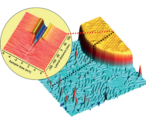
6. ŤĶįśüĽ„Éą„É≥„Éć„Éę„ÉĽ„ÉĚ„ÉÜ„É≥„ā∑„Éß„É°„Éą„É™„Éľ„Āę„āą„ā荰®ťĚĘťõĽśįóšľĚŚįé„ĀģÁ†ĒÁ©∂ (Surface conductivity studied by scanning tunneling potentiometry)
ŤĶįśüĽ„Éą„É≥„Éć„Éę„ÉĚ„ÉÜ„É≥„ā∑„Éß„É°„Éą„É™„Éľ„Ā®„ĀĮ„ÄĀŤ°®ťĚĘ„ĀģťõĽšĹć„ĀģÁ©ļťĖ܌łÉ„āíťĚ쌳ł„ĀęťęėÁ≤ĺŚļ¶„ĀꍙŅ„ĀĻ„āč„Āď„Ā®„ĀĆ„Āß„Āć„āčśł¨ŚģöśČčśģĶ„Āß„ÄĀŤ©¶śĖô„Āģšł°ÁęĮ„ĀęťõĽŚúß„āí„Āč„ĀĎ„Ā¶„ÄĀ„āľ„É≠„Éź„ā§„āĘ„āĻšĽėŤŅĎ„Āß„Éą„É≥„Éć„ÉęťõĽśĶĀ„ĀĆ„āľ„É≠„Āę„Ā™„āč„āą„ĀÜ„Āę„ÄĀśéĘťáĚԾ捩¶śĖôťĖď„Āģ„Éź„ā§„āĘ„āĻťõĽŚúß„āí„Éē„ā£„Éľ„ÉČ„Éź„ÉÉ„āĮŚą∂Śĺ°„Āô„āč„Āď„Ā®„Āę„āą„āä„ÄĀťõĽšĹć„āíśĪļŚģö„Āô„āč„Āď„Ā®„ĀĆ„Āß„Āć„āč„Äā„ĀĄ„Āö„āĆ„ĀĮ„Āď„Āģśł¨Śģöś≥ē„Ā®„āĻ„ÉĒ„É≥ŚĀŹś•ĶSTM„Ā®ÁĶĄ„ĀŅŚźą„āŹ„Āõ„Ā¶„ÄĀ„āĻ„ÉĒ„É≥śĶĀ„ĀģÁ©ļťĖ܌łÉ„ā퍙Ņ„ĀĻ„āč„Āď„Ā®„āíÁõģÁöĄ„Ā®„Āó„Ā¶Á†ĒÁ©∂„āíťÄ≤„āĀ„Ā¶„ĀĄ„Āĺ„Āô„Äā
Scanning tunneling potentiometry is a powerful tool to study surface conductivity in nanoscale. We are interested in surface conductivity of Si(111)-7×7, thin film, and topological materials. We are also interested in detection of spin current by the combination with spin-polarized STM in low temperature.
Á†ĒÁ©∂śąźśěúÔľö
M. Hamada and Y. Hasegawa,Phys. Rev. B 99, 125402 (2019).
M. Hamada and Y. Hasegawa, Jpn. J. Appl. Phys. 51, 125202 (2012)
„Ā™„Ā©